

Half of Nvidia
Half the cost of every Nvidia chip is no longer silicon
This is a briefing memo for the Curious Mind community. It reflects my personal views on a fast moving topic and is not a research report.
The most useful question I ask portfolio companies these days is no longer “how many GPUs can you get?” It is “how much HBM does your supplier have allocated to you for 2026?”
Most operators do not yet know the answer. The ones who do are the ones who will actually ship product.
For two years the bottleneck in the AI trade was clear and physical. TSMC could not produce enough advanced packages. The packages held the GPUs. The GPUs held the trade. Every quarter, the same phrase: we are supply-constrained. Then, sometime late last year, that constraint cleared. CoWoS (Chip-on-Wafer-on-Substrate) capacity tripled. Nvidia’s lead times shortened. The trade should have cooled.
It didn’t.
Because while the market was watching the foundry, the chokepoint had walked next door, to a small handful of memory companies most generalist investors still cannot spell. SK Hynix. Samsung. Micron. Three names that until recently were lumped together as a commodity cycle play, swinging between gluts and shortages every eighteen months. They are no longer commodity. The most expensive, most contested, most undersupplied component in the AI buildout is not the chip that does the math. It is the memory stacked next to it.
If you bought one of Nvidia’s latest accelerators today, roughly half of what you paid for would not be silicon doing logic. It would be memory.
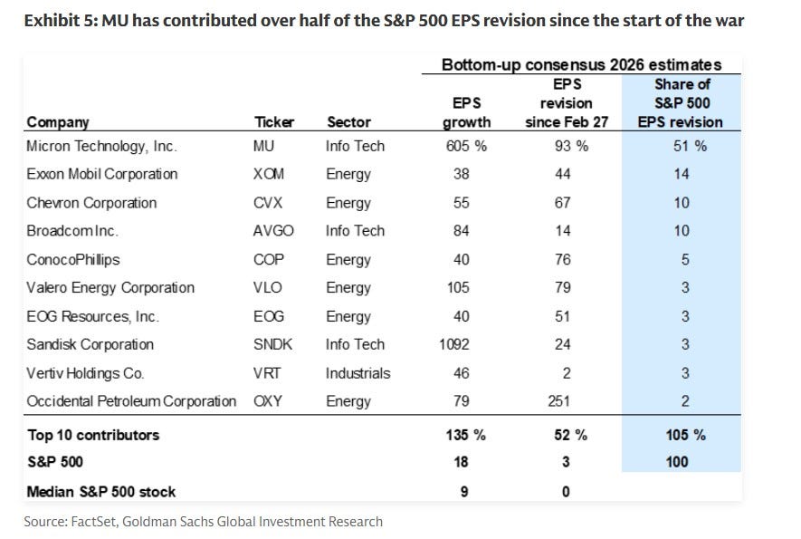
That number is the whole essay and explains why 50% of the S&P EPS revisions are coming from one company.
The Memory Wall
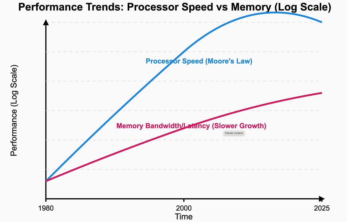
To understand why memory became the bottleneck, you have to understand a problem chip designers have been losing for two decades.
Processors have gotten faster every year. Memory has gotten faster too — but much slower than processors. The gap between what a chip can compute and what its memory can deliver has been widening since the early 2000s. Engineers call it the memory wall. By the late 2010s a top-end GPU could perform a calculation in a hundredth of the time it took to fetch the data for that calculation. The chip spent most of its life waiting.
For a while this didn’t matter. Most workloads, graphics, video, scientific simulation, could be tuned to keep data close at hand. You’d load a frame, do the work, write it back. The wall was real but you could plan around it.
Then came the transformer.
The defining feature of a modern AI model is that almost every operation requires a different slice of the model’s weights, sometimes hundreds of billions of parameters, to be available, right now, in milliseconds. There is no neat reuse pattern. There is no clever way to keep just the relevant bits close. You need everything, everywhere, all at once.
This is what people mean when they say AI is bandwidth-bound. It is not about how many calculations the chip can do per second. It is about how fast you can shovel the model’s weights through the chip’s mouth. A GPU that can do twenty thousand trillion operations a second is useless if its memory can only feed it the equivalent of three thousand. The other seventeen sit idle.
So the engineers did the only thing left.
They moved the memory inside the chip.
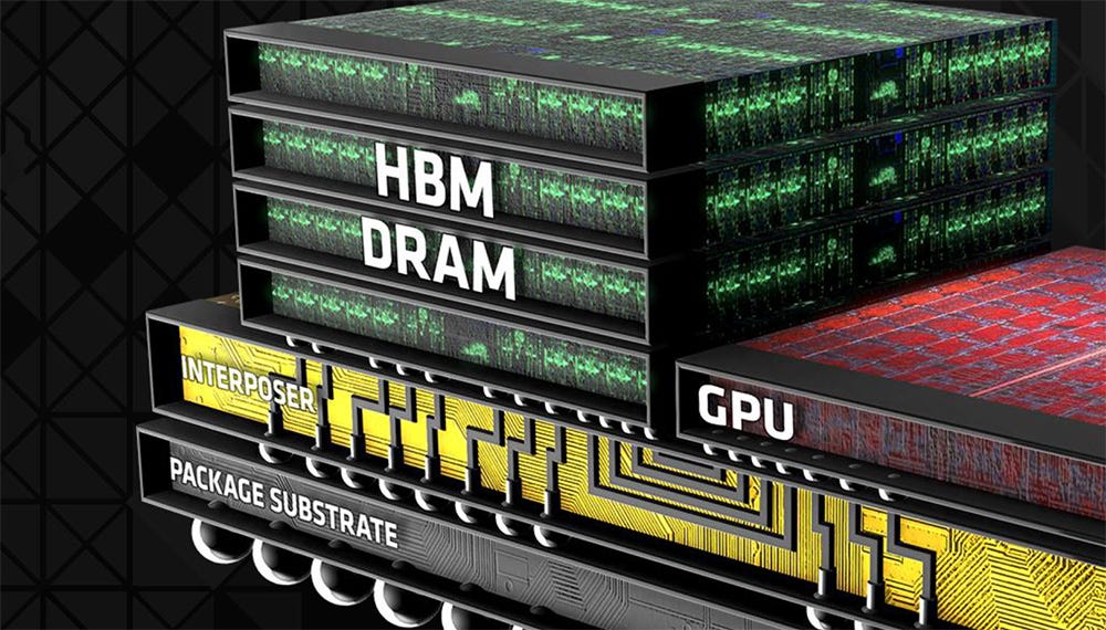
The Sandwich
A traditional computer puts memory on the motherboard, several inches from the processor, connected by skinny copper traces. The connection is fast in human terms and glacial in chip terms.
High Bandwidth Memory does three things differently.
First, it stacks the memory chips on top of each other, twelve, sometimes sixteen tall, and runs vertical wires straight through them, called through-silicon vias. Each finished stack contains as much memory as a small server.
Second, it sits the stack right next to the processor on a piece of silicon called an interposer. Not on the motherboard. Not even on the same circuit board. Glued onto the same package, millimeters away.
Third, it talks to the processor through thousands of parallel wires instead of a few dozen. The connection between a modern GPU and its memory is, quite literally, two thousand and forty-eight lanes wide. Imagine a highway that wide. That is the only way to keep the chip fed.
Each new HBM generation widens the highway and stacks more floors. HBM3 was the workhorse of 2024. HBM3E is most of what Nvidia is shipping now. HBM4, ramping through 2026, doubles the bandwidth again and brings something new — a bottom layer that is a small custom chip, made by a foundry like TSMC or Samsung, allowing the memory and the processor to be co-designed.
HBM is also only half the bottleneck. The other half is the interposer that the HBM and the GPU sit on, TSMC’s CoWoS process. You cannot ship one without the other, and the slower one in any given quarter sets the ship rate for Nvidia and AMD. When you read about Nvidia’s “supply” improving, what is usually clearing is one of these two, packaging or memory, and the other becomes the new gate. Watch them as a pair.
The line between memory and logic, between TSMC and Hynix, is dissolving. The “GPU” of 2027 will be honestly described as a memory-and-logic sandwich, where the memory is the heavier slice. The CPU — the boring brain I wrote about a few days ago, still sits on the motherboard with cheap commodity DDR5 next to it. That is fine. The CPU runs orchestration code that does not need this kind of feeding. But the workload that pays for the data center, model training and model inference, runs entirely on the memory-and-logic sandwich. And that sandwich is sold by exactly three companies on earth.
Jensen Huang has made the obvious counter publicly. The cost of materials inside an accelerator is a poor proxy for value capture. The architect of the system, the company that chose the memory, designed the interconnect, wrote the software, keeps the largest share. He is right. The memory maker still earns a strong margin on a strategic input. Both can be true. The question for the next two years is which margin compresses first.
The Ecosystem
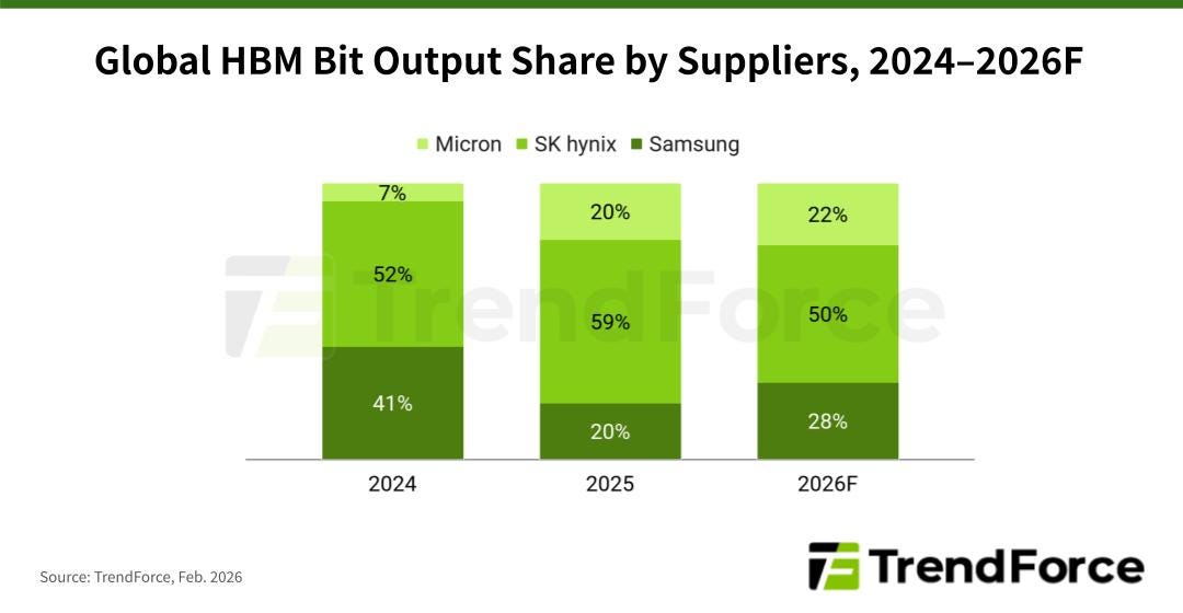
Until 2023, the global memory industry was a cyclical mess. Three players, SK Hynix, Samsung, and Micron, would race to add capacity, oversupply the market, watch prices collapse, cut capex, watch prices recover, and start the whole cycle again. HBM has rewired the cycle.
SK Hynix got there first and makes the bulk of the world’s HBM3E, including the memory inside Nvidia’s most-shipped accelerator. They were treated as a commodity stock for fifteen years. They are now the most important non-American technology company outside Taiwan. HBM margins are roughly three to five times what they earn on commodity DRAM. Around half their profits now come from a product that did not exist at scale four years ago.
The lead is worth understanding precisely. It is not a process lead at the cell level — all three players make competitive DRAM cells. It is a packaging and bonding lead. Stacking sixteen dies on top of each other with submicron alignment, and getting the thermal behavior right so the stack survives qualification, is hard. Yield is non-linear in stack height — going from 8-high to 12-high is much harder than 50% harder, and 16-high is where Samsung and Micron have stumbled. This is why bonding equipment from BESI and Disco matters so much for who wins the next two cycles.
Micron is the comeback story. They were late to HBM, lost share, and were left for dead in early 2024. Through 2025 and into this year they qualified into Nvidia’s supply chain at HBM3E, then announced HBM4 samples ahead of expectation. The stock has reflected the change. The question now is whether they can hold quality at HBM4, where the engineering challenge — particularly the bonding of stacked dies — is harder.
Samsung is the unresolved variable. They are the largest memory company in the world by volume and the slowest on HBM. They missed most of the HBM3E cycle. They have spent two years trying to qualify with Nvidia and have not. Their HBM4 pitch is ambitious, using their own foundry to make the bottom logic die, offering a fully integrated stack. If it works, the competitive map resets. If it does not, they spend another two years as a discount supplier.
Behind these three sit the picks and shovels. TSMC makes the interposer that the HBM stack and the GPU sit on (the CoWoS process), and packages the whole sandwich. ASML sells the lithography machines that make modern DRAM possible at all. Applied Materials and Lam Research sell the deposition and etch tools used in the stacking process.
The bonding and inspection layer is the most underappreciated piece of the equipment story. Disco and BE Semiconductor sell the equipment used to bond dies together with the right precision. Onto Innovation sells the metrology and inspection tools that verify the bonds held, every additional die in a stack means more inspection steps, and the equipment line item per HBM stack is growing faster than for any other DRAM product. Moving from HBM3 through HBM4 and beyond requires a transition from thermo-compression bonding to hybrid bonding, and the equipment makers who win that transition will earn through the entire cycle.
There is one adjacent trade worth a brief mention. As AI inference scales, the bottleneck spills beyond model weights into storage. Vector databases, retrieval-augmented generation, and KV-cache offload all require fast NAND-based storage tiered alongside HBM and DDR. Enterprise SSD demand has lifted as a result, and the NAND cycle is now running on its own version of the HBM dynamic — supply discipline, AI-driven demand pull, structural tightening. SanDisk is the cleanest large-cap exposure. It is a related trade rather than the same trade, but it sits inside the same physics: hot data in HBM, warm data in DDR, cold-but-still-fast data in enterprise NAND, and the price of all three rising at once.
This is not a list of recommendations. It is a map of who actually shows up at the loading dock when the AI trade buys HBM.
The New Cycle
You have probably seen the word memflation in some research note. It means what you think it means. The price of memory is rising, and rising in ways that are not behaving like a normal cycle.
Three things are different this time.
The first is mix. Each HBM stack consumes between two and three times as much wafer capacity as the equivalent number of bits of standard DRAM. That means even if memory companies wanted to satisfy both AI demand and traditional PC and server demand, they physically cannot. Every wafer they convert to HBM is a wafer of standard DRAM not made. The result is that the AI buildout is inflating the price of the memory in your laptop, your phone, your car. The strength in commodity DRAM pricing is miscast as a normal demand recovery — consumer and enterprise demand has been mediocre. What is happening is a manufactured shortage: the memory makers are starving the commodity book to prioritize HBM allocation. That joins two markets that used to move independently. Your laptop memory price is now a derivative of GPU shipments, and the commodity DRAM cycle no longer ends when supply catches up — it ends only when HBM demand cools.
The second is contracts. Memory has historically been a spot market. AI buyers, Nvidia, the hyperscalers, the sovereign labs, are now signing multi-year contracts at fixed-but-rising prices. SK Hynix has reported that all of their 2026 HBM capacity is sold. Samsung the same. Micron the same. The cycle has not been abolished, but the visibility into 2026 and most of 2027 is unlike anything memory has seen.
The third is capex discipline. The shortages of 2017 and 2018 ended with a rush of new fabs that crashed the market by 2019. This time the three players have been restrained. SK Hynix is adding capacity but at a measured pace. Samsung’s HBM4 ramp is constrained by yield, not by capex. Micron has guided that supply will lag demand into 2027.
How to Read the Headlines
A few practical filters for the news that will land in your inbox over the next year.
When you see “DRAM prices fell 4% in October” — this is almost always commodity DRAM, not HBM. HBM is contracted. The two markets are now mostly separate. The headline is real but it does not tell you what you think it does.
When you see “Samsung qualifies HBM3E with Nvidia” — read the fine print. Qualification can mean small volumes for a single SKU. The number that matters is what percentage of Nvidia’s shipped HBM is coming from each supplier. That number moves slowly.
When you see “Memory company announces $XX billion capex” — distinguish between brownfield expansion (existing fabs, fast to ramp) and greenfield (new fabs, two to three years out). Greenfield announcements rarely affect near-term supply but they reset the long-term cycle.
When you see “HBM4 yields disappointing at supplier X” — pay attention. The hardest engineering problem in HBM4 is bonding sixteen dies together with submicron precision. The first company to solve it at high yield wins the cycle. The companies that do not will lose share for two years.
What Would Break This
The HBM thesis rests on four things: that scaling laws keep working at the frontier, that inference stays bandwidth-bound, that the three players stay disciplined, and that no architectural shift reduces memory demand per unit of compute.
The scaling laws risk is the deepest because it is binary. Every assumption in this essay rests on the next generation of frontier models continuing to show capability gains as compute is scaled. If GPT-6, Claude 5, and Gemini 3 work, the demand picture for 2027 to 2029 is not what this essay implies. It is dramatically larger — sovereign labs, defense compute, and the corporate inference market all expand at once. If they do not work and the scaling era plateaus, demand collapses and the supply tightness this essay describes becomes a glut within eighteen months. The middle scenario — steady capex, manageable tightness — is the least likely outcome, not the most. The most important uncertainty in this trade is not cyclical. It is whether the largest scientific experiment in history continues to deliver.
The architecture risk is the next deepest. In-memory compute, optical interconnect, and 3D-stacked DRAM bonded directly onto the GPU die are all credible enough to take seriously. Optical in particular is already moving — Lumentum, Coherent, Astera Labs, and Credo are riding the same bandwidth-bound logic that lifted HBM, but at the rack-to-rack level rather than the chip-to-chip level. None of these is imminent as a full HBM substitute. All would, in different ways, dissolve the premium that today accrues to a stack of memory sitting next to a processor. If the workload itself changes, sparser models, mixture-of-experts, more efficient inference, bandwidth-per-FLOP requirements drop and the same HBM supply serves a much larger market. Good for AI economics. Bad for HBM pricing power.
The discipline risk is the most familiar. Three players have cooperated before, in 2017 and again in 2018, and cooperation has always broken. Samsung is the obvious crack point because they have the most share to recover and the largest underutilized capacity to throw at it. The moment they qualify HBM4 at scale and decide to underprice, the oligopoly margin structure resets.
The cycle timing risk is the simplest. Memory stocks have historically traded at terrible multiples in the back half of supply cycles even when earnings are still high, because the market prices the next downturn six to twelve months ahead. The fabs being announced today do not produce HBM tomorrow, but they produce it in 2027 and 2028. Memory cycles always overshoot. You can be right about HBM demand through 2027 and lose money in the stocks starting in mid-2026.
I am not making any of these calls today. The next twelve months look visible. But the smartest readers will close the tab thinking what’s missing is the other side. The other side is that this is a multi-condition bet dressed as a structural certainty, and the conditions deserve to be named.
The Strategic Layer
There is a layer above all of this that the cycle analysis does not capture. Two of the three HBM makers are South Korean. The third is American but small.
The most consequential industrial input to the American AGI program is manufactured almost entirely within range of Chinese missiles, in a country whose alignment with US technology controls is good but not permanent.
The CHIPS Act funding for Micron’s Idaho and New York expansion is the visible American response. The less visible response is the quiet conversation in Washington about whether HBM should be treated as strategic infrastructure, the way the US treats rare earths, pharmaceutical precursors, and certain refined metals, rather than as a commercial commodity. The answer to that question matters more for the 2028 trade than any of the cycle dynamics described above.
Watch the policy as carefully as you watch the players.
Coda
I asked a friend who runs supply chain for a large hyperscaler what kept him up at night. He said: “The chips. Always the chips.”
I asked which chips.
He paused.
“The memory. We can buy GPUs. We cannot buy memory.”
That conversation was six months ago. The HBM stocks have roughly doubled since. The structural story is not in the multiple. It is in the sentence my friend said. The single largest constraint on the most-watched technology buildout in history is being met by three companies. Two are foreign. One is American. None used to be considered strategic.
They are now.
And the friend’s sentence — we cannot buy memory — has started to mean something other than what it meant six months ago. It used to describe a procurement problem. It is becoming a national security problem.
If the GPU was the headline of the AI trade, the memory is the punchline. The punchline is doing more of the work than anyone wanted to admit. And it is being delivered by people most of the audience has never heard of, on a stage they did not know existed.
Watch the stack.
Disclaimer
This post is for informational and educational purposes only. It does not constitute investment advice, a recommendation, or an offer to buy or sell any security. I, members of my family, or entities I am associated with may hold positions in the companies or sectors discussed, and those positions may change at any time without notice. Past performance is not indicative of future results. You should consult your own financial, tax, and legal advisors before making any investment decision.
Appendix
Companies Mentioned (Map, Not Recommendations)
Memory makers
SK Hynix (KRX: 000660) — Korean, current HBM share leader
Samsung Electronics (KRX: 005930) — Korean, attempting to retake share at HBM4
Micron Technology (NASDAQ: MU) — American, the comeback story
Picks and shovels
TSMC (NYSE: TSM) — interposer and advanced packaging (CoWoS)
ASML (NASDAQ: ASML) — lithography for advanced DRAM
Applied Materials (NASDAQ: AMAT) — deposition and etch
Lam Research (NASDAQ: LRCX) — etch and stacking equipment
Disco Corporation (TYO: 6146) — wafer dicing and grinding
BE Semiconductor (AMS: BESI) — hybrid bonding equipment, key to HBM4 transition
Onto Innovation (NYSE: ONTO) — metrology and inspection for advanced packaging and HBM stacks
Optical and connectivity (the next layer out)
Lumentum (NASDAQ: LITE) — optical components for AI fabrics
Coherent (NYSE: COHR) — optical components and lasers
Fabrinet (NYSE: FN) — contract manufacturing for optical
Astera Labs (NASDAQ: ALAB) — connectivity controllers for AI clusters
Credo Technology (NASDAQ: CRDO) — high-speed connectivity ICs
Adjacent — storage
SanDisk (NASDAQ: SNDK) — enterprise NAND exposure to AI inference workloads
Buyers
Nvidia (NASDAQ: NVDA), AMD (NASDAQ: AMD) — the largest single customers
Hyperscalers (Amazon, Microsoft, Google, Meta) — direct buyers via custom silicon programs
Key Terms
HBM (High Bandwidth Memory) — vertically stacked DRAM placed adjacent to a processor on the same package
TSV (Through-Silicon Via) — vertical wires connecting stacked dies
Interposer — thin silicon substrate that connects HBM stacks to a GPU
CoWoS — TSMC’s advanced packaging process used for almost all current HBM-equipped GPUs
Memory bandwidth — how much data per second can be delivered between memory and processor
The memory wall — engineer’s term for the widening gap between processor speed and memory speed
DDR5 — current generation of standard server and PC memory (the kind in your laptop)
Hybrid bonding — die-to-die bonding technique required for HBM4 and beyond
CPO (Co-Packaged Optics) — moving data between chips as light rather than electrical signals, packaged onto the same substrate as the processor
NAND — non-volatile flash memory used for storage rather than working memory; the technology inside enterprise SSDs
Further Reading
These are the sources I returned to most while writing this. Where I have linked to a publication rather than a single piece, it is because the writer’s whole body of work matters more than any one essay.
The big-picture frame
Leopold Aschenbrenner, Situational Awareness: The Decade Ahead — situational-awareness.ai. The canonical argument for why the AI compute buildout is the most consequential industrial project of the century. Read the “From $1 Trillion Compute Cluster to Superintelligence” and “Racing to the Trillion-Dollar Cluster” sections in particular for the demand-side picture that sits underneath this essay.
Chris Miller, Chip War (2022) — the definitive book on the geopolitics of semiconductors. The chapters on Korea and Taiwan are essential context for the Strategic Layer argument here.
Ed Conway, Material World (2023) — broader frame on the physical inputs to the modern economy. The silicon chapter is a useful primer for non-specialists.
Ongoing primary research
SemiAnalysis (Dylan Patel and team) — semianalysis.com. The most important ongoing research on AI hardware, HBM supply chains, CoWoS bottleneck dynamics, and hyperscaler buildouts. Their pieces on the H100/H200/B200 BOM, the Samsung HBM qualification saga, and the CoWoS-S to CoWoS-L transition are each worth the subscription.
Stratechery (Ben Thompson) — stratechery.com. The strategic frame on Nvidia, TSMC, and the platform dynamics around AI compute.
Fabricated Knowledge (Doug O’Laughlin) — fabricatedknowledge.com. Long-form semiconductor analysis on Substack.
Digits to Dollars (Jay Goldberg) — digitstodollars.com. Industry-insider commentary, particularly strong on memory and packaging.
TrendForce — trendforce.com. The standard industry source for HBM market share and DRAM pricing data.
TechInsights — techinsights.com. The best teardown analyses of new accelerators.
Korean and Taiwanese press
ETNews (etnews.com) and KED Global (kedglobal.com) — earliest signals on Hynix and Samsung qualification timing.
Chosun Biz (biz.chosun.com) — Korean industrial policy and supplier dynamics.
DigiTimes (digitimes.com) — Taiwanese supply chain reporting, particularly on TSMC packaging capacity.
Primary source documents
SK Hynix, Micron, Samsung quarterly earnings calls — the SK Hynix call has become one of the most useful reads in semiconductors. Transcripts available at investor relations sites for each company.
TSMC quarterly earnings calls and CapEx commentary — the binding constraint on advanced packaging capacity.
Nvidia GTC keynotes (Jensen Huang) — for the customer side of the HBM demand picture.
Policy and national security
CSIS (Center for Strategic and International Studies) — csis.org. Their semiconductor supply chain reports are the best public-domain analysis of the strategic concentration question.
US Commerce Department CHIPS Act announcements — for the specific funding amounts and timelines for Micron’s domestic HBM ramp.
US Bureau of Industry and Security (BIS) export control filings — the policy lever most likely to reshape the HBM supply picture over the next two years.
Great summary of how memory changed with HBM and why this trend deserves a higher valuation multiple.
Great post! Nvidia is forming a monopoly in the AI space.